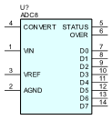
8-Bit Analog-to-Digital Converter
The ADC converts the analog voltage at input to an equivalent digital representation.
If the analog voltage at VIN is less than voltage at AGND, then all data pins are set to Low, and OVER pin is set to High. If the analog voltage at VIN exceeds the voltage at VREF then all data pins are set to High, and the OVER pin is set to High.
The sampling of the input voltage occurs on the rising edge of the CONVERT signal. Only one conversion is performed per rising edge. The Output pins go to the Unknown state and the STATUS pin goes to the High state TPCS seconds after the rising edge of the CONVERT signal. TPSD seconds later, the Output pins change to valid data. TPDS seconds later, the STATUS pin goes to the Low state.
Parameters
| Parameter | Description | Units | Default |
|---|---|---|---|
| TPCS | Time delay from rising edge of convert to rising edge of status. | s | DGTDELAY |
| TPSD | Time delay from rising edge of status to output and over-range signals. | s | DGTDELAY |
| TPDS | Time delay from output and over-range signals to falling edge of status. | s | DGTDELAY |
| OUT_MODE | Outputs mode. | OUT | |
| IOMODEL | The name of an I/O model, which describes the device’s loading and driving characteristics. | DGTDEFIOMODEL | |
| POWER_NODE | Digital power node name. Is the node used by the interface subcircuits which connect analog nodes to digital nodes. | $G_DPWR | |
| GROUND_NODE | Digital ground node name. Is the node used by the interface subcircuits which connect analog nodes to digital nodes. | $G_DGND |