16-Bit Shift Register with Clock Enable and Synchronous Reset
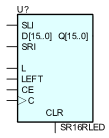
SR16RLED is a 16-bit shift register with shift-left (SLI) and shift-right (SRI) serial inputs, parallel inputs (D15 – D0), and four control inputs – clock enable (CE), load enable (L), shift left/right (LEFT), and synchronous reset (R). The register ignores clock transitions when CE and L are Low. The synchronous R, when High, overrides all other inputs and resets the data Q15 – Q0 outputs Low. When L is High and R is Low, the data on the D15 – D0 inputs is loaded into the corresponding Q15 – Q0 bits of the register. When CE is High and L and R are Low, data is shifted right or left depending on the state of the LEFT input. If LEFT is High, data on SLI is loaded into Q0 during the Low-to-High clock transition and shifted left (to Q1, Q2, and so forth) during subsequent clock transitions. If LEFT is Low, data on SRI is loaded into Q15 during the Low-to-High clock transition and shifted right (to Q14, Q13, and so forth) during subsequent clock transitions.
The default initial state of all flip-flops is zero.
Parameters
| Parameter | Description | Units | Default |
|---|---|---|---|
| DELAY | Propagation delay. | s | DGTDELAY |
| IN_MODE | Inputs mode. | IN | |
| OUT_MODE | Outputs mode. | OUT | |
| IOMODEL | The name of an I/O model, which describes the device’s loading and driving characteristics. | DGTDEFIOMODEL | |
| POWER_NODE | Digital power node name. Is the node used by the interface subcircuits which connect analog nodes to digital nodes. | $G_DPWR | |
| GROUND_NODE | Digital ground node name. Is the node used by the interface subcircuits which connect analog nodes to digital nodes. | $G_DGND |