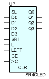
4-Bit Shift Register with Clock Enable and Asynchronous Clear
SR4CLED is a 4-bit shift register with shift-left (SLI) and shift-right (SRI) serial inputs, four parallel inputs (D3 – D0), and four control inputs – clock enable (CE), load enable (L), shift left/right (LEFT), and asynchronous clear (CLR). The register ignores clock transitions when CE and L are Low. The asynchronous clear, when High, overrides all other inputs and resets the data outputs (Q3 – Q0) Low. When L is High and CLR is Low, the data on the D3 – D0 inputs is loaded into the corresponding Q3 – Q0 bits of the register. When CE is High and L and CLR are Low, data is shifted right or left, depending on the state of the LEFT input. If LEFT is High, data on the SLI is loaded into Q0 during the Low-to-High clock transition and shifted left (to Q1, Q2, and so forth) during subsequent clock transitions. If LEFT is Low, data on the SRI is loaded into Q3 during the Low-to-High clock transition and shifted right (to Q2, Q1, and so forth) during subsequent clock transitions. The truth table indicates the state of the Q3 – Q0 outputs under all input conditions.
The default initial state of all flip-flops is zero.
Parameters
| Parameter | Description | Units | Default |
|---|---|---|---|
| DELAY | Propagation delay. | s | DGTDELAY |
| IN_MODE | Inputs mode. | IN | |
| OUT_MODE | Outputs mode. | OUT | |
| IOMODEL | The name of an I/O model, which describes the device’s loading and driving characteristics. | DGTDEFIOMODEL | |
| POWER_NODE | Digital power node name. Is the node used by the interface subcircuits which connect analog nodes to digital nodes. | $G_DPWR | |
| GROUND_NODE | Digital ground node name. Is the node used by the interface subcircuits which connect analog nodes to digital nodes. | $G_DGND |