This dialog box allows you to complete the configuration of the PCB by adding layers for base and finishing materials. It also allows you to configure layer pairs for PCB drilling.
 Note: Note: |
|---|
Before opening this dialog you must define all layers and views corresponding to the CAM outputs. See Creation and use of layers and views. |
 Tip: Tip: |
|---|
To open this dialog box, choose the Layers and Views command in the Settings menu or
if the Layer and View Bar is displayed, click the |
 button on the bar.
In the dialog box click on the button
button on the bar.
In the dialog box click on the button PCB Layer Stackup
The layers defined in the Layer Setup dialog box are listed in this box in their overlap order in the PCB. The layers relative to the base material of the PCB and any finishing layers of the board must be added to them.
To add a layer
-
Select the layer immediately adjacent to the layer to be added.
-
Click the Add button. The new layer is added above or below the selected layer.
- Index
-
Progressive index of copper layers.
- Type
-
Indicates the type of layer. The layer type is determined in the Layer Setup when the layer is created. Only for added layers you can set the type between: Core, Prepreg and Finish.
- Materials
-
Specify the material of which the layer is made.
- Thickness
-
Enter the thickness of the selected layer.
- CAM View
-
Select the view with which to generate the Gerber file for the layer.
- Notes
-
Specify any additional information.
Use vias
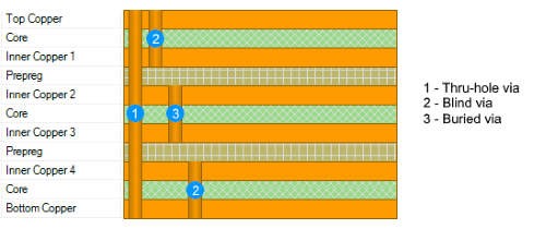
Vias are three-dimensional objects that have a copper area on each layer of the board with a central hole through it. They are used to form a vertical electrical connection between two or more electrical layers of a PCB. The most common type of vias is called thru-hole vias, which connects the two outer layers of the board. Blind vias and buried vias can also be used in multilayer boards. Blind vias join an outer layer of the board with an inner layer while buried vias join two inner layers of the board. The possible layers that a vias can cover depend on the manufacturing technology used to manufacture the board.
For multilayer PCBs, you can specify whether the board uses blind or buried vias. In this case, you must also create pairs of layers for drilling the PCB.
Drill pairs
Allows you to configure layer pairs for PCB drilling. Layer pairs for drilling must be configured when used blind or buried. A drilling pair must be defined for each pair of layers connected by the vias. This allows you to generate all the files needed to create the blind or buried vias for the production of the PCB.
Each drilling association consists of a start layer and a stop layer. The drilling pair obtained by matching the Top Copper layer to the Bottom Copper layer is predefined.
| Note: |
|---|
The pairs of layers for PCB drilling must be defined according to the construction method of the PCB. This should be done in consultation with the board manufacturer to ensure that the design matches their manufacturing technology. |
To add a pair
-
Click the Add button.
-
Select the start layer and stop layer from the top layer to the bottom layer.
To delete a pair
Select the pair to remove.
-
Click the Delete button. The drilling pair obtained by matching the Top Copper layer to the Bottom Copper layer is default and cannot be deleted.
IPC Level
This box allows you to select the construction level of the board according to the IPC-7351 specifications for the three-level library system. The different electronic products have different requirements of reliability, maintainability and density of the boards. With the concept of building the three-level library it is possible to generate footprints to meet these different needs by varying the pad size and the size of the component. For each device family, three variants are provided for pad geometry: Three pad geometry variants are provided for each device family: maximum pad size (low board density, level A), medium pad size (medium board density, level B) and minimum pad size (high board density, level C). See Drawing a three-level footprint.
| Note: |
|---|
When importing a footprint from libraries, the model corresponding to the PCB construction level set in this box is automatically selected. |