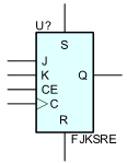
J-K Flip-Flop with Clock Enable and Synchronous Set and Reset
FJKSRE is a single J-K-type flip-flop with J, K, synchronous set (S), synchronous reset (R), and clock enable (CE) inputs and data output (Q). When synchronous set (S) is High, all other inputs are ignored and output Q is set High. (Set has precedence over Reset.) When synchronous reset (R) is High and S is Low, output Q is reset Low. When S and R are Low and CE is High, output Q responds to the state of the J and K inputs, as shown in the following truth table, during the Low-to-High clock (C) transition. When CE is Low, clock transitions are ignored. The default initial state of the flip-flop is zero.
| Inputs | Output | |||||
|---|---|---|---|---|---|---|
| S | R | CE | J | K | C | Q |
| 1 | X | X | X | X | ↑ | 1 |
| 0 | 1 | X | X | X | ↑ | 0 |
| 0 | 0 | 0 | X | X | X | No Chg |
| 0 | 0 | 1 | 0 | 0 | X | No Chg |
| 0 | 0 | 1 | 0 | 1 | ↑ | 0 |
| 0 | 0 | 1 | 1 | 0 | ↑ | 1 |
| 0 | 0 | 1 | 1 | 1 | ↑ | Toggle |
Parameters
| Parameter | Description | Units | Default |
|---|---|---|---|
| IC | Output initial state. | LOW | |
| CLKTPLH | Delay from clock to out high. | s | DGTDELAY |
| CLKTPHL | Delay from clock to out low. | s | DGTDELAY |
| PRETPLH | Delay from set to out high. | s | DGTDELAY |
| PRETPHL | Delay from set to out low. | s | DGTDELAY |
| CLRTPLH | Delay from reset to out high. | s | DGTDELAY |
| CLRTPHL | Delay from reset to out low. | s | DGTDELAY |
| IN_MODE | Inputs mode. | IN | |
| OUT_MODE | Outputs mode. | OUT | |
| IOMODEL | The name of an I/O model, which describes the device’s loading and driving characteristics. | DGTDEFIOMODEL | |
| POWER_NODE | Digital power node name. Is the node used by the interface subcircuits which connect analog nodes to digital nodes. | $G_DPWR | |
| GROUND_NODE | Digital ground node name. Is the node used by the interface subcircuits which connect analog nodes to digital nodes. | $G_DGND |