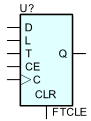
Toggle/Loadable Flip-Flop with Toggle and Clock Enable and Asynchronous Clear
When the asynchronous clear input (CLR) is High, all other inputs are ignored and output Q is reset Low. When load enable input (L) is High and CLR is Low, clock enable (CE) is overridden and the data on data input (D) is loaded into the flip-flop during the Low-to-High clock (C) transition. When toggle enable (T) and CE are High and L and CLR are Low, output Q toggles, or changes state, during the Low- to-High clock transition. When CE is Low, clock transitions are ignored.
Parameters
| Parameter | Description | Units | Default |
|---|---|---|---|
| IC | Output initial state. | LOW | |
| CLKTPLH | Delay from clock to out high. | s | DGTDELAY |
| CLKTPHL | Delay from clock to out low. | s | DGTDELAY |
| CLRTPLH | Delay from clear to out high. | s | DGTDELAY |
| CLRTPHL | Delay from clear to out low. | s | DGTDELAY |
| IN_MODE | Inputs mode. | IN | |
| OUT_MODE | Outputs mode. | OUT | |
| IOMODEL | The name of an I/O model, which describes the device’s loading and driving characteristics. | DGTDEFIOMODEL | |
| POWER_NODE | Digital power node name. Is the node used by the interface subcircuits which connect analog nodes to digital nodes. | $G_DPWR | |
| GROUND_NODE | Digital ground node name. Is the node used by the interface subcircuits which connect analog nodes to digital nodes. | $G_DGND |