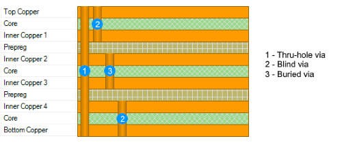
Vias are three-dimensional objects that have a copper area on each layer of the board with a central hole through it. They are used to create a vertical electrical connection between two or more electrical layers of a PCB. The most common type of vias is through-hole vias, which connects the two outer layers of the board. In multilayer boards, blind vias and buried vias can also be used. Blind vias join an outer layer of the board with an inner layer while buried vias join two inner layers of the board. The possible layers that a vias can connect depend on the manufacturing technology used to manufacture the board.
 Warning: Warning: |
|---|
The use of blind and buried vias must be enabled by defining layer pairs in the PCB Layer Stackup dialog box. A drilling pair must be defined for each pair of layers connected by the vias. This allows you to generate all the files needed to create the blind or buried vias for the production of the PCB. |
Commands for the object via
| Command | Description |
|---|---|
|
PCB » Via
|
Place a via in the drawing. |
