After transferring the information from the schematic to the PCB using the Schematic » Update PCB command, the list of components is visible in the PCB Panel and you can start placing them on the PCB.
 Note: Note: |
|---|
Component placement is a very important step in the whole PCB design process. The success of the next routing phase depends on it. |
Placing a component means having to specify its exact position on the PCB respecting the correct distances between the components and the design rules, but above all facilitating the subsequent routing phase of the PCB.
Choosing the view
Before starting to place components on the PCB it is useful to choose the best view, the one that gives us the most information for a simpler placement operation.
Visible Courtyard
The view must make visible the Courtyard layer relative to the side on which the components are to be placed.
A courtyard object is a closed polygon that defines the footprint profile of a component. The main use of a courtyard object is to provide the PCB designer with a guideline for positioning the footprint next to each other with sufficient space to compensate for component tolerances. This avoids any problems during the construction phase of the board.
All PCB models supplied with the program include the Top Coutyard and Bottom Courtyard views. In these views, the outline of the component is highlighted, including the minimum space required to be at the right distance from the other components.
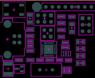
Visible Ratsnest
The view used to position the components on the PCB must make the set of connection lines visible. The connection lines are displayed on the Nets layer, so the view used for routing must include a Nets layer.
One way to find the best location for a component is to check the connection lines from the component pads to the pads of the other components on the PCB. Each component must be placed so as to minimize the length and intersection of these lines.
The Top Courtyard and Bottom Courtyard views include the Nets layer that shows the connection lines between the components. To set the display options of the connection lines, open the Layer Setup dialog and select the Nets layer in the current view.
Placement of components
After transferring the information from the circuit diagram to the PCB using the Schematic » Update PCB command, the list of components is visible in the PCB Panel and you can start placing them on the PCB.
To place a single component in the PCB
-
In the PCB Panel, click on the component name to select it. The cursor takes the form of a hand.
-
Click on the component name and drag it into the PCB. To rotate the component, press the R key.
To place all components on the document
All components can be placed on the document but outside the PCB profile. Subsequently, each component can be moved inside the PCB.
Choose the PCB » Routing » Auto Placer » Outside the PCB command or click on the tool
 in the toolbar.
All components are arranged on the sides of the PCB.
in the toolbar.
All components are arranged on the sides of the PCB.
To place components in the PCB, do one of the following:
Click on a component to select it and then drag it into the PCB. To rotate the component, press the R key.
Choose the command PCB » Routing » Auto Placer » Next Device, press the key combination CTRL+N or click on the tool
 in the toolbar.
The component is hooked to the mouse cursor and can be moved.
To rotate the component, press the R key.
in the toolbar.
The component is hooked to the mouse cursor and can be moved.
To rotate the component, press the R key.

To place all components inside the PCB
All components can be placed inside the PCB automatically. The automatic procedure places the components according to their geometry and the existing connections between the components. Subsequently, each component can be optimally repositioned.
Before performing the automatic placement, place all components that must occupy an exact position on the board and lock them to prevent them from being repositioned. For example, it is advisable to manually position all the connectors, transformers and, in general, all the bulky components. For how to block a component on the PCB see PCB Panel.
Choose the command PCB » Routing » Auto Placer » Inside the PCB or click on the tool
 in the toolbar.
The Auto Placer dialog box opens.
in the toolbar.
The Auto Placer dialog box opens.
| Note: |
|---|
The automatic placement of components on the PCB is a utility tool that cannot replace the experience and ability of a good designer. |